<< View SCS Blog
What Types of Materials can be Parylene Coated?
A large number of substrate surfaces can be coated with Parylene. Below is a sample list of several industrial applications that can be coated with Parylene conformal coatings.
- Printed circuit boards
- MEMs
- LEDs
- Catheters
- Stents
- Magnets
- Paper
- Needles
- Sensors
- Ferrite Cores
- Metallic Blocks
- Implantable devices
- Valves
- O-rings
- Tubing
- Silicon Wafers
- Keypads
- Stoppers
- Seals
- Mandrels
- Molds
- Motor Assemblies
- Optical lenses
- Power Supplies
- Backplanes
- Photoelectric Cells
- Forceps
- Test tubes
- Probes
- Fiber Optic Components
- Pace-makers
- Bobbins
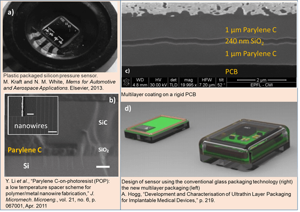
With Parylene chemical vapor deposition (CVD), it is possible to obtain stress-free and defect-free conformal coatings on almost all types of materials. Sensors used in the automotive industry can be prone to high temperatures, hydrocarbons and moisture. Such environments cause the sensor’s aluminum contact pads to corrode quickly. Parylene conformal coatings help protect the sensor from these harsh environments. Parylene is also used as a masking material in MEMS devices due to its capability to fill the crevices. In image A below, it fills under the undercut and acts as a spacer to produce 100 nm wide nanowires (inset). The study shows it forms interfaces with a polymeric resist, Silicon, Silicon Carbide and Platinum [2]. Images C and D demonstrate that the Parylene can be applied to replace the glass packaging leading to a smaller dimension and weight in the package. Also, the Parylene can be coated as a stack of layers combined with other thin layers such as SiO2 as shown in image C. The diversity in the applications and possibilities makes the Parylene a very attractive conformal coating.
However, there are a few steps to follow before starting the deposition process. To prevent delamination, pinholes, cracks, wrinkles, blisters and other types of thin film defects different types of surfaces require different surface preparations.
Example Parylene/Material Systems:
- PCB: The most common application area of Parylene is PCBs as a protective coating of the electronic components, bonds and the wires. It forms a protective layer against mechanical impact and diffusion of corrosive elements [11].
- Silicon Wafer: Wafer bonding intermediate layers [12], as a mask for silicon chemical etching [13].
- Ceramic / Glass: A-174 silane solution pretreatment can improve the adhesion of the Parylene C thin film on flat glass substrate specimens [14].
- Metals / Alloys: Parylene is widely used in coating sensor pads. (Image A shows a plastic packaged silicon pressure sensor [1]) Parylene suffers from poor adhesion to itself and noble metals, such as gold and platinum. To promote their adhesion a commercially available adhesion promoter can be used and it was reported that a 100-fold increase in adhesive strength at such interfaces was achieved and the corresponding improvements in resistance to moisture driven delamination were observed [15].
- Parylene – Metal – Parylene: Sandwich structures are produced as flexible electrodes, sensors, in general as biocompatible implants [16]–[18].
- Parylene – Parylene: Deposition is possible but requires post-treatment to form a chemically stable interface by thermal treatment [16], [19].
- Polymers: Parylene C on photoresist can be achieved by improving the adhesion of the resist and Parylene introducing a modified silanization pretreatment including heat treatment to remove hydroxyl groups from the surface of the resist. [2]
- On Oil: When the vapor pressure of the oil is low (<5 Pa) it is possible to deposit Parylene on top[3]. Parylene coated on oil exhibits a small stress and it can be ignored [4]. Parylene-on-oil deposition (CVD) has been used for the preparation of long-term implantable pressure sensors [5], optical lenses out of oil [6]–[8] and to make isolated Parylene films by separating the Parylene after deposition [9], [10].
References
[1] M. Kraft and N. M. White, Mems for Automotive and Aerospace Applications. Elsevier, 2013.
[2] Y. Li et al., “Parylene C-on-photoresist (POP): a low temperature spacer scheme for polymer/metal nanowire fabrication,” J. Micromechanics Microengineering, vol. 21, no. 6, p. 067001, Apr. 2011, doi: 10.1088/0960-1317/21/6/067001.
[3] A. Homsy et al., “Solid on liquid deposition, a review of technological solutions,” Microelectron. Eng., vol. 141, pp. 267–279, Jun. 2015, doi: 10.1016/j.mee.2015.03.068.
[4] “Tensile Film Stress of Parylene Deposited on Liquid | Langmuir.” https://pubs.acs.org/doi/10.1021/la102790w (accessed Apr. 26, 2020).
[5] A. M. Shapero, Y. Liu, and Y.-C. Tai, “Parylene-on-oil packaging for long-term implantable pressure sensors,” Biomed. Microdevices, vol. 18, no. 4, p. 66, Jul. 2016, doi: 10.1007/s10544-016-0089-4.
[6] Binh-Khiem Nguyen, Eiji Iwase, Kiyoshi Matsumoto, and Isao Shimoyama, “Electrically driven varifocal micro lens fabricated by depositing Parylene directly on liquid,” in 2007 IEEE 20th International Conference on Micro Electro Mechanical Systems (MEMS), Jan. 2007, pp. 305–308, doi: 10.1109/MEMSYS.2007.4433059.
[7] T. Kan, H. Aoki, N. Binh-Khiem, K. Matsumoto, and I. Shimoyama, “Ratiometric Optical Temperature Sensor Using Two Fluorescent Dyes Dissolved in an Ionic Liquid Encapsulated by Parylene Film,” Sensors, vol. 13, no. 4, pp. 4138–4145, Apr. 2013, doi: 10.3390/s130404138.
[8] W. F. Gorham, “A New, General Synthetic Method for the Preparation of Linear Poly-p-xylylenes,” J. Polym. Sci. [A1], vol. 4, no. 12, pp. 3027–3039, 1966, doi: 10.1002/pol.1966.150041209.
[9] H. Keppner and M. Benkhaira, “Method for producing a plastic membrane device and the thus obtained device,” US20090246546A1, Oct. 01, 2009.
[10] N. Binh-Khiem, K. Matsumoto, and I. Shimoyama, “Porous Parylene and effects of liquid on Parylene films deposited on liquid,” in 2011 IEEE 24th International Conference on Micro Electro Mechanical Systems, Jan. 2011, pp. 111–114, doi: 10.1109/MEMSYS.2011.5734374.
[11] A. Hogg, “Development and Characterisation of Ultrathin Layer Packaging for Implantable Medical Devices,” p. 219.
[12] H. Noh, K. Moon, A. Cannon, P. J. Hesketh, and C. P. Wong, “Wafer bonding using microwave heating of Parylene intermediate layers,” J. Micromechanics Microengineering, vol. 14, no. 4, pp. 625–631, Apr. 2004, doi: 10.1088/0960-1317/14/4/025.
[13] Hsi-wen Lo, Wen-Cheng Kuo, Yao-Joe Yang, and Yu-Chong Tai, “Recrystallized Parylene as a mask for silicon chemical etching,” in 2008 3rd IEEE International Conference on Nano/Micro Engineered and Molecular Systems, Jan. 2008, pp. 881–884, doi: 10.1109/NEMS.2008.4484464.
[14] “The Adhesion Properties of Parylene-C Thin Films | Scientific.Net.” https://www.scientific.net/AMM.421.337 (accessed Apr. 26, 2020).
[15] “Characterization and Modification of Adhesion in Dry and Wet Environments in Thin-Film Parylene Systems – IEEE Journals & Magazine,” Accessed: Apr. 26, 2020. [Online]. Available: https://ieeexplore.ieee.org/abstract/document/8418313.
[16] R. P. von Metzen and T. Stieglitz, “The effects of annealing on mechanical, chemical, and physical properties and structural stability of Parylene C,” Biomed. Microdevices, vol. 15, no. 5, pp. 727–735, Oct. 2013, doi: 10.1007/s10544-013-9758-8.
[17] W. Li, D. C. Rodger, E. Meng, J. D. Weiland, M. S. Humayun, and Y.-C. Tai, “Flexible Parylene Packaged Intraocular Coil for Retinal Prostheses,” in 2006 International Conference on Microtechnologies in Medicine and Biology, May 2006, pp. 105–108, doi: 10.1109/MMB.2006.251502.
[18] S. Minnikanti et al., “Lifetime assessment of atomic-layer-deposited Al2O3-Parylene C bilayer coating for neural interfaces using accelerated age testing and electrochemical characterization,” Acta Biomater., vol. 10, no. 2, pp. 960–967, Feb. 2014, doi: 10.1016/j.actbio.2013.10.031.
[19] J. Ortigoza-Diaz et al., “Techniques and Considerations in the Microfabrication of Parylene C Microelectromechanical Systems,” Micromachines, vol. 9, no. 9, Aug. 2018, doi: 10.3390/mi9090422.