<< View SCS Blog
What Happens to Parylene when the Dielectric Voltage is Exceeded?
Parylenes, derived from poly(para-xylylene), serve as conformal coatings across diverse sectors like automotive, medical, electronics, military and semiconductor industries. They are inert, transparent and have excellent barrier properties as dielectric thin films. Because their deposition takes place under vacuum, sub-micron range crevices can be coated leading to excellent barrier properties (void free) and they have extraordinary purity that is of great importance in electronic applications. Not all Parylene derivatives show the same dielectric properties (Table 1). It is also important to note that dielectric properties of Parylenes depend on their thickness thus their % crystallinity which is explained below.
| Parylene N | Parylene C | Parylene F | |
| Molecular structure | |||
| Chemical Formula | C16H16 | C16H14Cl2 | C16H8F8 |
| Optical | Transparent | Transparent | Transparent |
| Biocompatibility | Yes | Yes | Yes |
| Electrical Properties | |||
| Dielectric Strength V/mil | 7000 | 5600 | 6800 |
| Dielectric Constant 1 MHz 1 KHz 60 Hz | 2.65 2.65 2.65 | 2.95 3.10 3.15 | 2.17 |
| Volume Resistivity ohm•cm | 1.40 x 10¹⁷ | 8.80 x 10¹⁶ | 2.0 x 10¹⁷ |
Before, diving into Parylenes some general definitions would be helpful to explain what dielectric strength and breakdown voltage is. Dielectric strength of a polymeric material can be defined as the measure of dielectric breakdown resistance under an applied voltage (Dielectric strength is calculated by dividing the breakdown voltage by the thickness of the sample.). It is expressed as Volts per unit thickness. The higher the value, the more electrically insulating a material is. Technically, insulators do not conduct electricity but if the electric field is large enough, the insulator breaks down and conducts electricity [1].
Once the breakdown voltage is exceeded physically the polymer may burn or punctures can occur that will conduct electricity[2]. It must be kept in mind that the thickness of an insulating material plays a role in determining its breakdown voltage and it is not linear.
Parylene derivatives are partially crystalline [3], [4]. Deposition rate, thickness, post-deposition thermal treatment affects the crystallinity of Parylenes [3], [5]. As reported by Kahouli, the dielectric constant of Parylene C increases as a power law according to film thickness ε′ = dβ with β = 0.042 ± 0.04 for d < 1000 nm and 0.0138 ± 0.02 for d > 1000. This was attributed to the decreasing number of voids and discontinuities of the material with increasing film thickness. The significance of this study is that normally the electrical properties of thin films are speculated from their bulk samples. This study reports the dielectric properties of the Parylene C films on substrates with film thicknesses of 40–83000 nm. It was reported that the polymer becomes semi-crystalline above 40 nm thickness. Critical film thickness was measured as 1000 nm and below this critical thickness the dielectric constant decreases below the bulk value [3]. Figure 1 shows the thickness vs dielectric constant dependency.
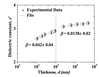
Figure 1: Dielectric constant of Parylene-C as a function of thickness [3]
In another study, Parylene C was measured for its electrical breakdown voltage on a 2 mm × 2 mm area capacitor structure where it acted as a dielectric layer as illustrated in Figure 2. Results have shown that Parylene C has excellent electrical properties, particularly in terms of its dielectric strength. Its breakdown voltage was reported to remain constant across the entire capacitor area, which is typical for uniform and pinhole-free layers. The above results show that thin Parylene C films are good candidates for the gate insulating material in microelectronic applications[5]. In a different study, breakdown voltage was studied
for Parylene C and they showed that the breakage results in deformation of the Parylene layer forming bubbles in the film (Figure 3) [6]
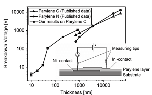
Figure 2: Thin Parylene C layers breakdown voltage as a function of their thickness [5].
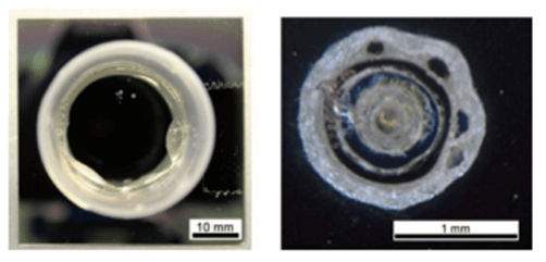
Figure 3: Sample after measurement: close up of a defect in the Parylene C layer where the breakdown appeared (Parylene thickness of 1.9 µm) [6].
References
[1] “How to Calculate Breakdown Voltage,” Sciencing. [Online]. Available: https://sciencing.com/calculate-breakdown-voltage-6728339.html. [Accessed: 20-Dec-2022].
[2] “Dielectric Strength: Units, Test Methods & Material Table.” [Online]. Available: https://omnexus.specialchem.com/polymer-properties/properties/dielectric-strength. [Accessed: 20-Dec-2022].
[3] A. Kahouli, “Effect of film thickness on structural, morphology, dielectric and electrical properties of Parylene C films,” J. Appl. Phys., vol. 112, no. 6, p. 064103, Sep. 2012, doi: 10.1063/1.4752022.
[4] W. R. Dolbier and W. F. Beach, “Parylene-AF4: a polymer with exceptional dielectric and thermal properties,” J. Fluor. Chem., vol. 122, no. 1, pp. 97–104, Jul. 2003, doi: 10.1016/S0022-1139(03)00100-3.
[5] T. Marszalek, M. Gazicki-Lipman, and J. Ulanski, “Parylene C as a versatile dielectric material for organic field-effect transistors,” Beilstein J. Nanotechnol., vol. 8, no. 1, pp. 1532–1545, Jul. 2017, doi: 10.3762/bjnano.8.155.
[6] A. Heid, R. von Metzen, A. Stett, and V. Bucher, “Examination of dielectric strength of thin Parylene C films under various conditions,” Curr. Dir. Biomed. Eng., vol. 2, no. 1, Jan. 2016, doi: 10.1515/cdbme-2016-0012.