<< View SCS Blog
How Fast Does Parylene Deposit?
Parylene conformal coatings combine a number of properties that are attractive for use in a wide spectrum of applications. Their low dielectric properties, high mechanical strength, transparency, bio compatibility, chemical inertness against all of the common acids, bases and organic solvents, low water/gas permeability and thermal properties make them interesting for use in many industries. Also, pinhole-free Parylene conformal coatings with a thickness higher than 0.1 μm are possible and have been reported earlier [1]. Therefore, understanding their deposition process and characteristics is important.
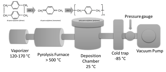
Parylene conformal coatings are deposited using the Gorham chemical vapor deposition (CVD) process under vacuum. The CVD process of Parylene takes place in three steps (sublimation, pyrolysis, deposition) as shown in the Figure. First the dimer (precursor with two repeating units) is sublimed. Next step the dimer is cracked into two monomers by pyrolysis at temperatures above > 500°C. Finally, the monomers polymerize on the substrate surface (as well as chambers surfaces) forming linear polymer chains. This final step takes place at room temperature and stress free conformal coatings are obtained.
Factors Affecting the Parylene Deposition Rate and Thickness:
The deposition rate and the pressure of Parylene conformal coatings during coating process controls uniformity and surface roughness of the final thin film. High pressure and high deposition rate have been reported to yield rough and non-uniform thin film coatings with poor dielectric properties [1]. Jui-Mei Hsu et al reported that high precursor sublimation rates resulted in slightly higher root-mean-square surface roughnesses from 5.78 to 9.53 nm for deposition rates from 0.015 to 0.08 g/min [2]. Therefore, extra care must be taken when choosing the deposition rate which in turn affects how fast the Parylene can be deposited.
According to Franz Selbmann et al, Eq. (1) and (2) shows that the Parylene thickness s and the deposition duration t increase with increasing dimer mass (amount of dimer used) by a factor of about 0.45 µm/g and 10.80 min/g, respectively. They worked with dimer masses between 1.1 g to 10 g to find a correlation. All depositions were performed at:
- 130°C sublimation temperature and autogenous pressure <5.5 Pa.
- s = 0.3386 µm + 0.4528 µm/g · mD (Eq 1)
- t = 1.55 min + 10.80 min/g · mD (Eq 2)
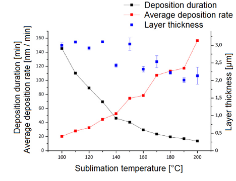
They explored various deposition parameters to assess their impact on the Parylene coatings. By adjusting the sublimation temperature from 100°C to 200°C in 10°C increments, they observed a deposition rate ranging from 20 nm/min at 100°C to 156 nm/min at 200°C. They also showed that the layer thickness was slightly lower for higher sublimation temperatures which was explained by the lower dwell time and the lower reaction time of the monomer molecules [2].
While Parylene coatings are typically thin, they also deposit relatively slowly. The fastest-depositing variant of Parylene — Parylene C — typically deposits at a rate of 0.2 mils or 5 microns per hour. This means that a 75 micron coating would take approximately 15 hours. Parylene N and D deposit more slowly.
The duration of the process can vary, ranging from a few hours to more than 24 hours, contingent upon the desired coating thickness. Factors such as dimer mass, deposition rate and temperature influence the time needed to achieve this specific thickness.
References
[1] T. Marszalek, M. Gazicki-Lipman, and J. Ulanski, “Parylene C as a versatile dielectric material for organic field-effect transistors,” Beilstein J. Nanotechnol., vol. 8, no. 1, pp. 1532–1545, Jul. 2017, doi: 10.3762/bjnano.8.155.
[2] F. Selbmann, M. Baum, M. Wiemer, and T. Gessner, “Deposition of Parylene C and characterization of its hermeticity for the encapsulation of MEMS and medical devices,” in 2016 IEEE 11th Annual International Conference on Nano/Micro Engineered and Molecular Systems (NEMS), Sendai, Japan, Apr. 2016, pp. 427–432, doi: 10.1109/NEMS.2016.7758283.